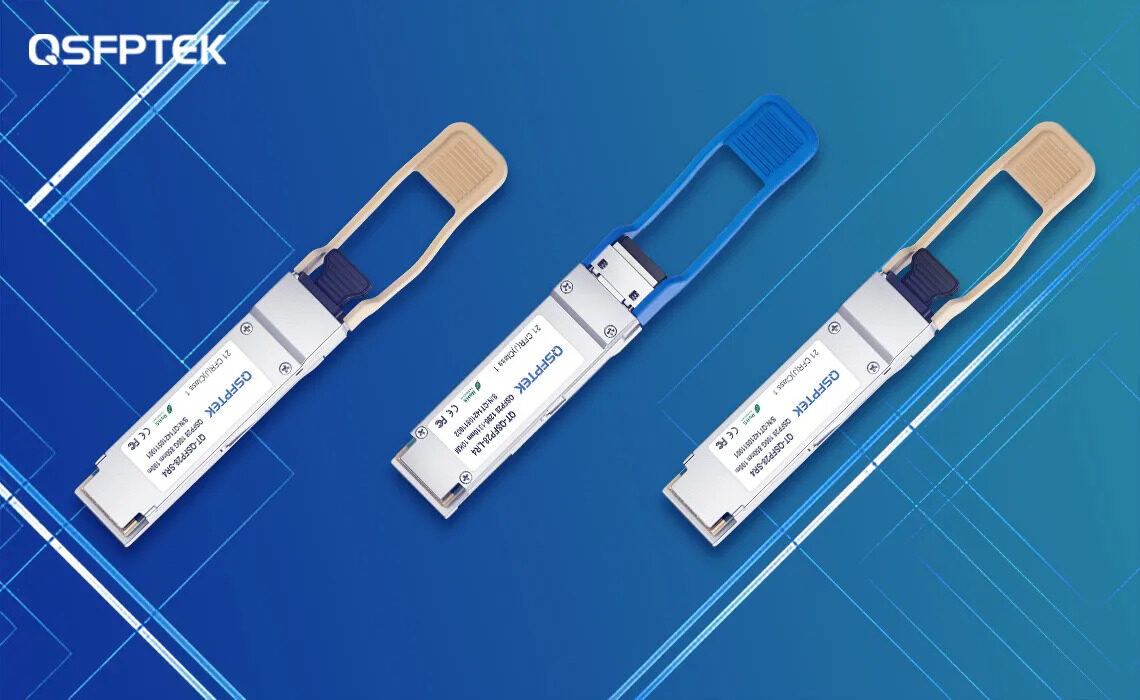
The optical module is one of the core components of the optical fiber communication system and the most important part of the optical communication equipment. Its main function is to realize the conversion of optical and electrical signals. With the development of the Internet, the amount of network data increases exponentially, and the construction of Internet data centers drives the growth of the optical module market. As one of the basic components of network construction, optical modules are very critical in the entire network construction.
The packaging form of optical modules is also constantly evolving, the volume is changing in a smaller and smaller direction, and the speed, power consumption, distance, cost, and other aspects are also constantly moving forward. This article focuses on the key points of optical module processing and manufacturing process control, and how to manage and control such products from the design, technical, and quality aspects.
Special requirements for optical module PCB processing
Table of Contents
Optical module products generally have the following characteristics according to the processing characteristics. The structure contains mixed pressure (high frequency + FR-4 or high speed + FR-4), controlled depth milling, high-precision impedance lines, small spacing between connecting pads, buried copper blocks or buried Special features such as ceramics, fine lines, long and short or graded board edge headers, various back drilled holes, precise alignment, precision bond pads, nickel palladium gold, etc.
Key Quality Standards for Optical Module Products
1. The corrosion resistance of the plug
The industry-accepted standard is that the plug and bond area need to pass the porosity, salt spray test, nitric acid gas test, and mixed gas (high-end product requirement) test.
2. Plug surface quality requirements
Because the signal is transmitted on the surface, it is not allowed to expose copper, nickel, palladium, or black spots; surface scratches, uneven defects, copper bumps & copper particles, pinholes, and nicks are not allowed; the surface roughness must be within the control range.
3. Dimensional tolerance requirements
Plug length and width tolerance control: ±0.1mm; plug center to board edge tolerance control: ±0.05 mm; plug distance tolerance control: ±0.05 mm; card slot diameter tolerance control: ±0.05 mm; card slot to plug center tolerance control: ±0.1 mm.
4. Bonding performance requirements
Bonding pad size: ≥75 μm; bonding strength of 20 μm width gold wire ≥4 g; bleed ability control.
Key Process Control of Optical Module Products

Image source: https://www.fiberopticshare.com/
1. Plug surface dent control
- There should be no scratches, pits, scratches, residual glue, and other defects on the surface of the laminated steel plate.
- Use a sticky cloth to pre-clean the fused board surface before arranging the board.
- Use 35 μm copper foil as the isolation film to arrange the board (the smooth surface must be clean).
- Insert the clapboard when removing the board.
- Using X-ray drilling + automatic cutting and grinding line production.
- The vacuum degree must be controlled in the drilling to prevent any dust between the cover plate or the plate and the plate.
- Grinding treatment before electroplating must ensure that there is no scratching on the board surface.
2. Control of copper nodules on the plug surface
- VCP electroplating + low current density production.
- Rough grinding and fine grinding surface treatment must be carried out after electroplating.
- It is produced by using a ceramic brush roller grinding line.
3. Brush mark defect control on the plug surface
- Pre-processing of graphic transfer: Ultra-roughening treatment does not allow mechanical grinding.
- Pre-treatment of printed resist plating oil: pumice powder treatment cannot be mechanically brushed.
- Secondary dry film pre-treatment: sandblasting, no grinding.
As the core device for photoelectric conversion in optical communication, optical modules are widely used in data centers. Data centers not only require high-speed 40G, 100G optical modules and above but also require continuous evolution in network architecture to achieve non-blocking network performance.
This article is a set of technical data summed up by the author based on his own experience in making optical module PCBs and by consulting relevant materials, hoping to be helpful to the industry.


No Comments